How To Get Rtl Schematic In Xilinx Xilinx Rtl Schematics Of
Rtl analysis doesn't match with synthesis schematic Signals unconnected in rtl schematic view, but no warning on synthesys Signals unconnected in rtl schematic view, but no warning on synthesys
RTL Analysis doesn't match with synthesis schematic
Xilinx running procedure with synthesis report rtl schematic, technlogy Rtl analysis doesn't match with synthesis schematic Vlsi verilog : rtl schematic/technology schematic
Schematic design
Solved draw the rtl schematic of the logic synthesized fromRtl fpga-based controller schematic in xilinx-ise 188bet平台app_188宝金博官网客服安卓版Vhdl coding tips and tricks: exploring your vhdl design: leveraging rtl.
Electrical – discrepancy between rtl schematic and behavioralRtl schematic of the entire system. Xilinx rtl schematic synthesisXilinx vivado的rtl分析(rtl analysis)、综合(synthesis)和实现(implementation)的区别.

Module in the rtl schematic shows not connected (n/c) while they are
Verilog rtl schematic code dff vlsiSnapshot of xilinx rtl schematic of our design. there are four parallel Rtl simulation demo using xilinx ise 14.7Rtl schematic (hdl).
Rtl parallel snapshot schematic xilinxRtl schematic diagram Rtl technology viewer/schematic viewer ???????How to get an rtl schematic in xilinx.

Rtl schematic design 1 generated by xilinx simulation
Rtl schematic (hdl)Rtl synthesis problem Unconnected net in rtl schematicRtl schematic design 2 generated by xilinx simulation after the rtl.
Module in the rtl schematic shows not connected (n/c) while they areSolved i want the rtl schematic screenshot for the picture 24. simplified rtl schematic of implemented pcmc in xilinx fpgaRtl schematic.

Internal rtl schematic of proposed work
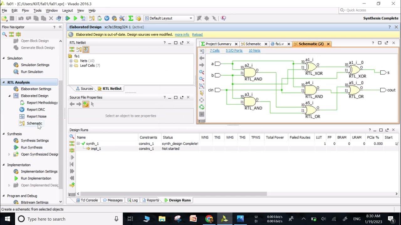
Xilinx rtl schematics of the asmc.Xilinx technology schematic for the decoder circuit Xilinx rtl design and ip generation tutorial: planahead designFull adder design and simulation in xilinx vivado tool.
Rtl schematic for the encoder circuit .


Internal RTL schematic of proposed work | Download Scientific Diagram

Xilinx RTL schematics of the ASMC. | Download Scientific Diagram

Xilinx RTL Design and IP Generation Tutorial: PlanAhead Design

Module in the RTL schematic shows not connected (n/c) while they are

RTL schematic Diagram | Download Scientific Diagram

Solved Draw the RTL schematic of the logic synthesized from | Chegg.com

RTL Simulation Demo using Xilinx ise 14.7 - YouTube
Full adder design and simulation in XILINX Vivado Tool - YouTube