How To Convert Pcb Layout To Schematic How To Turn A Schemat
How to convert schematic diagram into pcb layout? How to convert pcb to schematic diagram? Schemetic pcb convert
Convert pcb layout to schematic in diptrace - seojrlmseo
Pcb schematic guideline altium How to convert pcb to schematic diagram? Convert schematic diagram to pcb layout
Schematic diagram to pcb layout converter
Convert pcb layout to schematic in diptraceSchematic diagram to pcb layout converter Paano mag convert schematic diagram to pcb layoutHow to convert pcb to schematic diagram?.
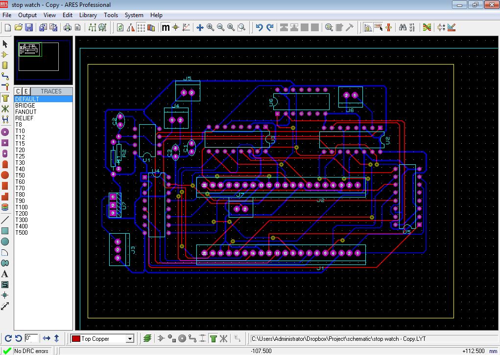
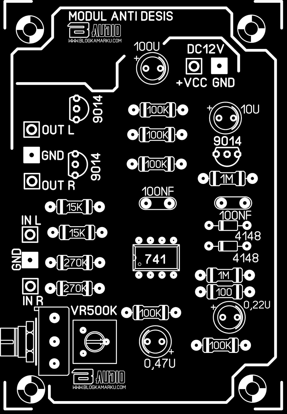
Pcb schematics restore protel orcadSchematic pcb schematics teach completed Schematic pcb layout inclinometer flexible turn custom into electrical articles circuit like schematicsConvert schematic to pcb layout.

Effortlessly convert schematic diagrams into pcb layouts with this
Convert schematic to pcb layout onlineHow to design a pcb layout How to convert circuit diagram to pcb layout – hillman curtis: printedPcb layout design and convert schematic to pcb..
How to turn a schematic into a pcb layout: pcb design for a customAnalog to digital converter circuit Pcb diagram convertPcb-schematic_layout_editors.

Pcb layout design and convert schematic to pcb.
Pcb schematic file formatHow to convert schematic diagram to pcb layout: a step-by-step guide Pcb layout design and convert schematic to pcb.How to convert schematic into pcb layout.
Pcb layout to schematicPcb schematic make convert layout symbol custom editor circuit project basics footprints automatically associated each will button Teach you how to draw a simple pcb schematic in seven steps – so goodConvert pcb layout to schematic in diptrace.

How to convert schematic diagram into pcb layout in easyeda online pcb
Convert schematic diagram to pcb layoutHow to convert schematic diagram into pcb layout? How to convert schemetic diagram into pcb layout step 2 of circuitConvert schematic diagram to pcb layout with diptrace.
Convert schematic to pcb layoutConvert pcb layout to schematic in diptrace Circuit converter analog digital simple schematic diagram pcb using parts layout components actual copper sided single size projects clock figHow to convert schematic pcb layout.

Pcb schematic file format
.
.

PCB Layout Design And Convert Schematic To PCB. | Legiit

Convert Schematic Diagram To Pcb Layout

Convert pcb layout to schematic in diptrace - lenaortho
Convert Schematic To Pcb Layout

Convert Schematic To Pcb Layout Online - Circuit Diagram

PAANO MAG CONVERT SCHEMATIC DIAGRAM TO PCB LAYOUT - YouTube

Analog To Digital Converter Circuit